- 您现在的位置:买卖IC网 > Sheet目录364 > SST49LF008A-33-4C-EIE-T (Microchip Technology)IC FLASH FWH 8MBIT 33MHZ 40TSOP
�� �
�
�8� Mbit� Firmware� Hub�
�A� Microchip� Technology� Company�
�SST49LF008A�
�Data� Sheet�
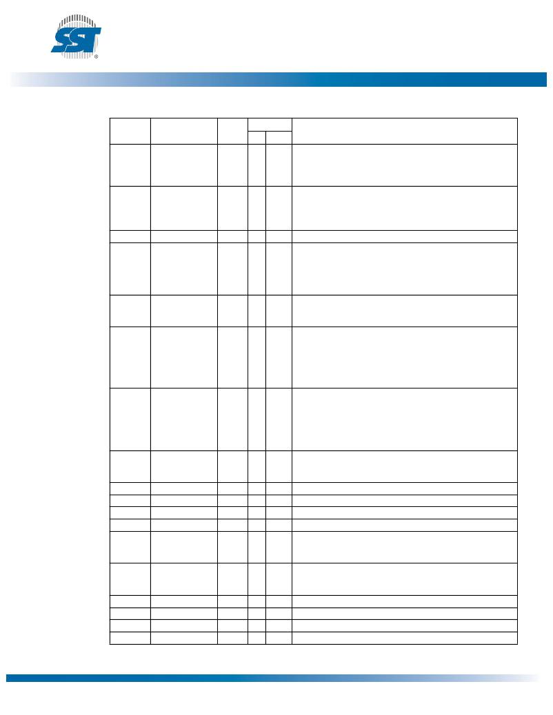
�Table� 1:� Pin� Description�
�Interface�
�Symbol�
�Pin� Name�
�Type� 1� PP� FWH� Functions�
�A� 10� -A� 0�
�Address�
�I� X�
�Inputs� for� low-order� addresses� during� Read� and� Write� opera-�
�tions.� Addresses� are� internally� latched� during� a� Write� cycle.� For�
�the� programming� interface,� these� addresses� are� latched� by� R/�
�C#� and� share� the� same� pins� as� the� high-order� address� inputs.�
�DQ� 7� -DQ� 0� Data�
�I/O�
�X�
�To� output� data� during� Read� cycles� and� receive� input� data� during�
�Write� cycles.� Data� is� internally� latched� during� a� Write� cycle.� The�
�outputs� are� in� tri-state� when� OE#� is� high.�
�OE#�
�WE#�
�Output� Enable�
�Write� Enable�
�I�
�I�
�X�
�X�
�To� gate� the� data� output� buffers�
�To� control� the� Write� operations�
�IC�
�Interface�
�I�
�X�
�X�
�This� pin� determines� which� interface� is� operational.� When� held�
�Configuration�
�Pin�
�high,� programmer� mode� is� enabled� and� when� held� low,� FWH�
�mode� is� enabled.� This� pin� must� be� setup� at� power-up� or� before�
�return� from� reset� and� not� change� during� device� operation.� This� pin�
�is� internally� pulled-� down� with� a� resistor� between� 20-100� K� ??�
�INIT#�
�Initialize�
�I�
�X�
�This� is� the� second� reset� pin� for� in-system� use.� This� pin� is� inter-�
�nally� combined� with� the� RST#� pin;� If� this� pin� or� RST#� pin� is�
�driven� low,� identical� operation� is� exhibited.�
�ID[3:0]�
�Identification�
�I�
�X�
�These� four� pins� are� part� of� the� mechanism� that� allows� multiple�
�Inputs�
�parts� to� be� attached� to� the� same� bus.� The� strapping� of� these�
�pins� is� used� to� identify� the� component.The� boot� device� must�
�have� ID[3:0]=0000� and� it� is� recommended� that� all� subsequent�
�devices� should� use� sequential� up-count� strapping.� These� pins�
�are� internally� pulled-down� with� a� resistor� between� 20-100� K� ??�
�FGPI[4:0]� General� Pur-�
�pose� Inputs�
�I�
�X�
�These� individual� inputs� can� be� used� for� additional� board� flexibil-�
�ity.� The� state� of� these� pins� can� be� read� through� GPI_REG� regis-�
�ter.� These� inputs� should� be� at� their� desired� state� before� the� start�
�of� the� PCI� clock� cycle� during� which� the� read� is� attempted,� and�
�should� remain� in� place� until� the� end� of� the� Read� cycle.� Unused�
�GPI� pins� must� not� be� floated.�
�TBL#�
�Top� Block� Lock�
�I�
�X�
�When� low,� prevents� programming� to� the� Boot� Block� sectors� at� top� of�
�memory.� When� TBL#� is� high� it� disables� hardware� write� protection� for�
�the� top� block� sectors.� This� pin� cannot� be� left� unconnected.�
�FWH[3:0]�
�CLK�
�FWH4�
�FWH� I/Os�
�Clock�
�FWH� Input�
�I/O�
�I�
�I�
�X�
�X�
�X�
�I/O� Communications�
�To� provide� a� clock� input� to� the� control� unit�
�Input� Communications�
�RST#�
�WP#�
�Reset�
�Write� Protect�
�I�
�I�
�X�
�X�
�X�
�To� reset� the� operation� of� the� device�
�When� low,� prevents� programming� to� all� but� the� highest� address-�
�able� blocks.� When� WP#� is� high� it� disables� hardware� write� protec-�
�tion� for� these� blocks.� This� pin� cannot� be� left� unconnected.�
�R/C#�
�Row/Column�
�I�
�X�
�Select� For� the� Programming� interface,� this� pin� determines� whether�
�Select�
�the� address� pins� are� pointing� to� the� row� addresses,� or� to� the� column�
�addresses.�
�RES�
�Reserved�
�X�
�These� pins� must� be� left� unconnected.�
�V� DD�
�V� SS�
�NC�
�Power� Supply�
�Ground�
�No� Connection�
�PWR�
�PWR�
�I�
�X�
�X�
�X�
�X�
�X�
�X�
�To� provide� power� supply� (3.0-3.6V)�
�Circuit� ground� (OV� reference)� All� V� SS� pins� must� be� grounded.�
�Unconnected� pins�
�T1.4� 25085�
�1.� I� =� Input,� O� =� Output�
�?2011� Silicon� Storage� Technology,� Inc.�
�6�
�DS25085A�
�10/11�
�发布紧急采购,3分钟左右您将得到回复。
相关PDF资料
SST49LF016C-33-4C-EIE-T
IC FLASH SER LPC 16MBIT 40TSOP
SST49LF080A-33-4C-WHE-T
IC FLASH SER LPC 8MBIT 32TSOP
SST49LF160C-33-4C-NHE
IC FLASH SER LPC 16MBIT 32PLCC
ST40
DIAC 35-45V BILATERAL TRIG DO214
STRIKER
SURGE SUPPRESSR 120V 7OUT 6'CORD
SUPER-7
SURGE SUPPRESSOR 7 OUT 7' CORD
SUPER6TEL12
SURGE SUPPR 7OUT 12'CORD W/RJ11
SUPER6TEL
SURGE SUPPRESSOR 7OUT W/TEL
相关代理商/技术参数
SST49LF008A-33-4C-NH
制造商:SST 制造商全称:Silicon Storage Technology, Inc 功能描述:2 Mbit / 3 Mbit / 4 Mbit / 8 Mbit Firmware Hub
SST49LF008A-33-4C-NHE
功能描述:闪存 8M (1Mx8) 33MHz Commercial Temp RoHS:否 制造商:ON Semiconductor 数据总线宽度:1 bit 存储类型:Flash 存储容量:2 MB 结构:256 K x 8 定时类型: 接口类型:SPI 访问时间: 电源电压-最大:3.6 V 电源电压-最小:2.3 V 最大工作电流:15 mA 工作温度:- 40 C to + 85 C 安装风格:SMD/SMT 封装 / 箱体: 封装:Reel
SST49LF008A-33-4C-NHE_
制造商:Microchip Technology Inc 功能描述:
SST49LF008A-33-4C-NHE-T
功能描述:闪存 8M (1Mx8) 33MHz 3.0-3.6V Commercial RoHS:否 制造商:ON Semiconductor 数据总线宽度:1 bit 存储类型:Flash 存储容量:2 MB 结构:256 K x 8 定时类型: 接口类型:SPI 访问时间: 电源电压-最大:3.6 V 电源电压-最小:2.3 V 最大工作电流:15 mA 工作温度:- 40 C to + 85 C 安装风格:SMD/SMT 封装 / 箱体: 封装:Reel
SST49LF008A-33-4C-NHE-T-CUT TAPE
制造商:Microchip 功能描述:SST49LF Series 8 Mbit 1024 K x 8 3.3 V Firmware Hub - PLCC-32
SST49LF008A-33-4C-WH
制造商:SST 制造商全称:Silicon Storage Technology, Inc 功能描述:2 Mbit / 3 Mbit / 4 Mbit / 8 Mbit Firmware Hub
SST49LF008A-33-4C-WHE
功能描述:闪存 8 MBIT FIRMWARE HUB RoHS:否 制造商:ON Semiconductor 数据总线宽度:1 bit 存储类型:Flash 存储容量:2 MB 结构:256 K x 8 定时类型: 接口类型:SPI 访问时间: 电源电压-最大:3.6 V 电源电压-最小:2.3 V 最大工作电流:15 mA 工作温度:- 40 C to + 85 C 安装风格:SMD/SMT 封装 / 箱体: 封装:Reel
SST49LF008A-33-4C-WHE_
制造商:Microchip Technology Inc 功能描述: